Photolithography Equipment Market Outlook and Forecast
The Photolithography Equipment Market continues to play a pivotal role in the global semiconductor manufacturing ecosystem, serving as a foundational technology for integrated circuit fabrication. The increasing demand for advanced chips across artificial intelligence, high-performance computing, automotive electronics, consumer devices, and industrial automation is driving investments in photolithography technologies. As chipmakers strive to achieve smaller node sizes and higher transistor densities, the adoption of advanced lithography systems remains a strategic priority across the semiconductor value chain.
2025 Market Size: USD 13.11 Billion
Projected 2035 Market Size: USD 24.61 Billion
Growth Forecasts (2026–2035): 6.5%
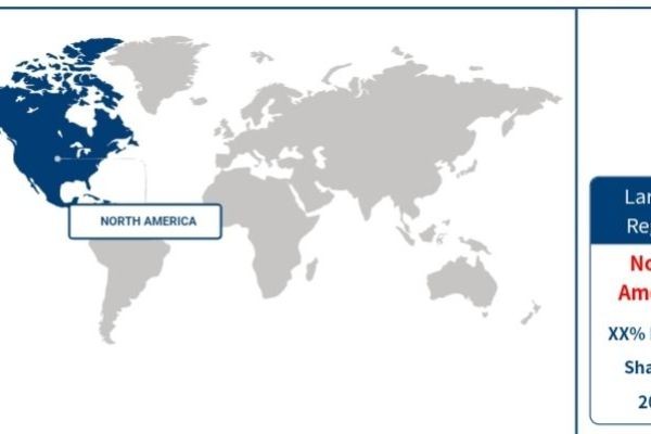
Regional Performance Highlights
North America remains a significant contributor to the photolithography equipment market due to robust semiconductor research activities, government-backed manufacturing initiatives, and the presence of leading chip designers and technology innovators. Continued investments in domestic semiconductor production facilities are strengthening regional demand for advanced lithography equipment.
Europe maintains a strong market position through its advanced semiconductor ecosystem, precision engineering expertise, and strategic investments in semiconductor sovereignty. The region's focus on automotive electronics and industrial automation continues to support photolithography equipment deployment.
Asia Pacific dominates the market owing to extensive semiconductor manufacturing operations in countries such as Taiwan, South Korea, China, and Japan. The concentration of wafer fabrication facilities and ongoing capacity expansion projects make the region the largest consumer of photolithography equipment globally.
Market Segment Analysis
Integrated Device Manufacturers (IDMs) represented the leading end-user segment, accounting for 57.68% of the market in 2025. These organizations benefit from vertically integrated operations that require continuous investments in advanced lithography systems to enhance production efficiency and technological competitiveness.
Deep Ultraviolet (DUV) technology dominated the market with a 51.5% share in 2025. DUV systems continue to be widely utilized across multiple semiconductor manufacturing processes due to their established infrastructure, cost efficiency, and capability to support high-volume chip production.
Request Free Sample Report @ https://www.fundamentalbusinessinsights.com/request-sample/14920
Top Market Trends Transforming the Photolithography Equipment Industry
1. Growing Adoption of Advanced Semiconductor Manufacturing Nodes
Semiconductor manufacturers are increasingly transitioning toward advanced process nodes to support AI processors, data center applications, and next-generation consumer electronics. This shift is driving demand for sophisticated photolithography systems capable of delivering higher precision, improved patterning accuracy, and enhanced throughput. Investments in cutting-edge fabrication facilities worldwide are accelerating technology upgrades across lithography platforms.
2. Expansion of Artificial Intelligence and High-Performance Computing Applications
The rapid growth of AI workloads and high-performance computing environments is generating significant demand for advanced semiconductors. To manufacture increasingly complex chips, foundries are expanding their use of advanced photolithography technologies that enable higher transistor densities and improved chip performance. This trend continues to create opportunities for equipment manufacturers and technology suppliers.
3. Increasing Government Support for Semiconductor Localization
Governments worldwide are implementing initiatives to strengthen domestic semiconductor manufacturing capabilities. Public and private sector investments in new fabrication plants are driving procurement of photolithography equipment. National strategies focused on supply chain resilience and technological independence are further stimulating market growth.
4. Integration of Automation and Smart Manufacturing Technologies
Modern semiconductor fabrication facilities are increasingly incorporating automation, predictive maintenance, and data-driven process optimization. Photolithography equipment manufacturers are integrating advanced software capabilities, real-time monitoring systems, and artificial intelligence tools to improve operational efficiency, reduce downtime, and enhance production quality.
Request Free Sample Report @ https://www.fundamentalbusinessinsights.com/request-sample/14920
Recent Company Developments
ASML Holding
ASML continues to strengthen its leadership position in advanced lithography by expanding production capacity and enhancing its portfolio of high-performance lithography systems. The company remains focused on supporting growing semiconductor manufacturing demand through continuous innovation and strategic customer collaborations.
Nikon Corporation
Nikon has continued investing in semiconductor manufacturing technologies, emphasizing improvements in lithography system performance, productivity, and precision. The company is pursuing opportunities across advanced packaging and semiconductor fabrication applications.
Canon Inc.
Canon has advanced its lithography solutions portfolio through technology enhancements designed to improve manufacturing efficiency and support evolving semiconductor production requirements. The company remains active in serving both mature and advanced semiconductor markets.
Ultratech (Veeco Instruments)
Veeco has continued expanding its semiconductor equipment capabilities through investments in process technologies that support advanced packaging and wafer-level manufacturing. The company's initiatives align with increasing demand for high-performance semiconductor devices.
SCREEN Semiconductor Solutions
SCREEN has focused on expanding its semiconductor equipment offerings, introducing solutions that improve fabrication productivity and yield management. The company continues to benefit from ongoing investments in semiconductor manufacturing facilities globally.
Tokyo Electron Limited (TEL)
Tokyo Electron remains a major participant in semiconductor manufacturing equipment markets, pursuing technology advancements that complement lithography processes and improve wafer fabrication efficiency. The company has expanded support for next-generation semiconductor production requirements.
KLA Corporation
KLA continues to invest in process control and inspection technologies that enhance photolithography precision and manufacturing quality. The company's innovations help semiconductor manufacturers achieve higher yields and optimize advanced production processes.
Applied Materials
Applied Materials has strengthened its semiconductor manufacturing solutions portfolio through strategic investments in materials engineering and process technologies. The company supports advanced semiconductor fabrication through integrated equipment and software solutions.
Lam Research
Lam Research continues expanding its capabilities across semiconductor manufacturing processes, developing technologies that improve pattern transfer accuracy and production efficiency. Its solutions support the growing complexity of advanced semiconductor devices.
Samsung Electronics Semiconductor Division
Samsung has increased investments in advanced semiconductor manufacturing infrastructure, driving demand for next-generation photolithography equipment and supporting innovation across memory and logic chip production.
Request Free Sample Report @ https://www.fundamentalbusinessinsights.com/request-sample/14920
Opportunities and Challenges in the Photolithography Equipment Market
The photolithography equipment market presents substantial opportunities driven by semiconductor demand growth, AI-driven computing requirements, automotive electrification, and next-generation communication technologies. Expanding fabrication capacity across major semiconductor-producing regions continues to create a favorable environment for equipment suppliers.
However, the industry also faces challenges. High equipment costs, complex manufacturing requirements, supply chain constraints, and increasing technological sophistication can create barriers for market participants. Additionally, geopolitical considerations and semiconductor trade restrictions may influence investment decisions and technology deployment strategies.
Despite these challenges, continued innovation, strong demand for advanced chips, and sustained investments in semiconductor manufacturing infrastructure position the photolithography equipment market for long-term development and technological advancement.
Request Free Sample Report @ https://www.fundamentalbusinessinsights.com/request-sample/14920
Related Reports
About Fundamental Business Insights:
Fundamental Business Insights is global market research and consulting company which is engaged in providing in depth market reports to its various types of clients like industrial sectors, financial sectors, universities, non-profit, and corporations. Our goal is to offer the correct information to the right stakeholder at the right time, in a format that enables logical and informed decision making. We have a team of consultants who have experience in offering executive level blueprints of markets and solutions. Our services include syndicated market studies, customized research reports, and consultation.
Contact us:
Robbin Fernandez
Head of Business Development
Fundamental Business Insights and Consulting
Email: sales@fundamentalbusinessinsights.com


