Photomask for Lithography Market, Trends, Business Strategies 2025-2032
The global Photomask for Lithography Market size was valued at US$ 5.67 billion in 2024 and is projected to reach US$ 9.23 billion by 2032, registering a CAGR of 7.3% during the forecast period 2025-2032. The U.S. Photomask for Lithography market accounted for USD 1.5 billion in 2024, while China is expected to grow at a faster pace, reaching USD 2.1 billion by 2032. The quartz photomask segment, which held over 60% market share in 2024, is anticipated to maintain its dominance with projected revenues of USD 4.3 billion by 2032.
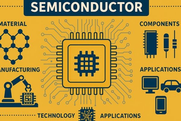
Photomasks are critical components in semiconductor manufacturing that transfer circuit patterns onto silicon wafers during lithography processes. These precision quartz or glass plates contain microscopic patterns that define the circuitry for integrated circuits. The technology has evolved to meet shrinking node requirements, with advanced masks now supporting features below 10nm. Main product categories include binary masks, phase-shift masks, and EUV masks – each serving different semiconductor Photomask for Lithography market needs.
The Photomask for Lithography market growth is driven by rising semiconductor demand across consumer electronics, automotive, solar applications, and IoT devices. However, increasing R&D costs for advanced nodes and the complexity of EUV mask production pose challenges for manufacturers. Leading Photomask for Lithography market companies such as Photronics and Toppan are investing in next-generation solutions and expanding production capacity to meet the growing demand.
The competitive landscape is concentrated, with the top five Photomask for Lithography manufacturers market share accounting for about 65% of global capacity in 2024. The Photomask for Lithography reclaim market and Photomask for Lithography market price trends are also influencing procurement strategies in the semiconductor market.
Overall, the Photomask for Lithography market forecast 2025-2032 indicates robust opportunities for manufacturers, driven by advancements in semiconductor lithography technology, increasing chip complexity, and the need for high-precision photomasks to support cutting-edge nodes.
Our comprehensive Market report is ready with the latest trends, growth opportunities, and strategic analysis. https://semiconductorinsight.com/download-sample-report/?product_id=107977
Segment Analysis:
By Type
Quartz Photomask Segment Dominates Due to High Precision and Durability in Advanced Lithography
The photomask market is segmented based on material type into:
- Quartz Photomask
- Subtypes: Fused silica masks, synthetic quartz masks
- Soda Photomask
- Others
- Subtypes: Chromium masks, emulsion masks
By Application
EUV Lithography Segment Leads as Semiconductor Industry Moves to Smaller Node Processes
The market is segmented by application into:
- EUV Lithography
- DUV Lithography
- Subtypes: KrF lithography, ArF lithography
By End User
Foundries Segment Dominates as Chip Manufacturing Drives Demand
The market is segmented by end user into:
- Semiconductor Foundries
- IC Design Houses
- Memory Manufacturers
- Others
By Technology Node
Sub-10nm Segment Growing Strongly as Industry Moves to Advanced Nodes
The market is segmented by technology node into:
- >45nm
- 28-45nm
- 10-28nm
- <10nm
Regional Analysis: Photomask for Lithography Market
North America
The North American photomask market is driven by strong semiconductor industry demand, particularly in the U.S. where companies like Intel and GlobalFoundries continue to invest in advanced fabrication facilities. The CHIPS and Science Act, which allocated $52 billion for domestic semiconductor manufacturing, is accelerating demand for high-precision photomasks, especially for EUV lithography applications. While quartz photomasks dominate due to their durability and thermal stability, there is growing interest in advanced mask technologies to support sub-7nm node production. California’s Silicon Valley and Arizona’s expanding semiconductor hubs remain key consumption centers, supported by proximity to major foundries and R&D facilities.
Europe
Europe maintains a stable photomask market, primarily serving automotive and industrial semiconductor applications. Germany leads in demand due to its robust automotive electronics sector, while the Netherlands benefits from ASML’s EUV technology leadership. The EU’s €43 billion Chips Act has intensified focus on domestic semiconductor production, creating opportunities for photomask suppliers. However, the region faces challenges including higher production costs compared to Asian counterparts and limited advanced node capacity. European manufacturers are increasingly adopting multi-beam mask writing technologies to improve productivity, though market growth remains moderate compared to other regions.
Asia-Pacific
Asia-Pacific dominates the global photomask market, accounting for over 60% of worldwide demand. China’s aggressive semiconductor self-sufficiency push, backed by $150 billion in planned investments through 2030, is driving massive photomask consumption. Taiwan and South Korea remain critical hubs, home to TSMC and Samsung’s advanced foundries that require cutting-edge mask technologies. Japan retains strong presence in mask blank production with companies like Hoya and Toppan. While cost sensitivity keeps soda lime masks prevalent for mature nodes, quartz photomasks are gaining traction for advanced applications. India’s emerging semiconductor ecosystem also presents new growth opportunities, though infrastructure limitations currently constrain faster adoption.
South America
South America’s photomask market remains nascent but shows gradual growth potential. Brazil leads regional demand, primarily serving consumer electronics and automotive sectors through imported semiconductor components. Local photomask production is minimal, with most supply coming from North American and Asian manufacturers. Economic instability and limited domestic semiconductor manufacturing have constrained market development, though recent incentives for electronics production in Mexico could stimulate regional growth. The market predominantly uses basic photomask technologies for mature process nodes, with advanced lithography applications remaining limited to multinational corporations with local operations.
Middle East & Africa
The Middle East currently represents a small but strategically emerging market for photomasks, particularly in Israel and UAE-based semiconductor initiatives. Israel’s strong fabless semiconductor ecosystem creates steady demand for photomask services, while Saudi Arabia’s $6 billion semiconductor investment plan signals long-term potential. Africa’s market remains negligible, though South Africa shows modest activity in legacy semiconductor applications. The region overwhelmingly relies on imports, with limited local mask production capabilities. As sovereign wealth funds increasingly target technology investments, the market may see accelerated growth, particularly for basic photomask needs in consumer electronics manufacturing.
List of Key Photomask for Lithography Companies Profiled
- Photronics (PKL) (U.S.)
- Toppan Printing Co., Ltd. (Japan)
- Dai Nippon Printing Co., Ltd. (Japan)
- Hoya Corporation (Japan)
- SK-Electronics Co., Ltd. (South Korea)
- LG Innotek (South Korea)
- ShenZheng QingVi (China)
- Taiwan Mask Corporation (Taiwan)
- Nippon Filcon Co., Ltd. (Japan)
- Compugraphics Photomask Solutions (UK)
The global semiconductor industry’s relentless growth is a primary driver for the photomask market, as these precision templates are indispensable for chip manufacturing. With semiconductor revenues projected to surpass $1 trillion by 2030, the need for advanced photomasks is increasing exponentially. The transition to smaller process nodes (below 7nm) requires more complex mask designs, with the average number of masks per wafer rising from 60 in 2020 to over 100 for cutting-edge nodes. This technological evolution is creating sustained demand for high-quality photomasks across foundries and IDMs worldwide.
Extreme Ultraviolet (EUV) lithography represents a paradigm shift in semiconductor manufacturing, requiring entirely new photomask technologies. As leading foundries expand EUV adoption for 5nm and below nodes, the EUV photomask market is experiencing rapid growth. These specialized masks demand ultra-smooth, defect-free substrates with multilayer reflective coatings, creating opportunities for manufacturers who can meet these stringent requirements. The push for improved resolution and overlay accuracy in advanced nodes is further driving innovation in photomask technologies and materials.
Recent global semiconductor supply chain disruptions and trade tensions are prompting countries to develop domestic photomask production capabilities. Governments worldwide are implementing initiatives to strengthen semiconductor sovereignty – from the CHIPS Act in the United States to similar programs in Europe and Asia. These policies are driving significant investments in regional photomask manufacturing facilities, with capital expenditures for new mask shops increasing by over 30% annually since 2021.
The development of advanced patterning technologies beyond EUV presents significant opportunities for photomask innovators. High-NA EUV systems require novel mask architectures with fundamentally different optical properties. Additionally, experimental approaches like nanoimprint lithography and directed self-assembly are spurring research into alternative mask types. Companies developing these next-generation solutions stand to capture substantial market share as the industry explores post-EUV technologies.
The shift towards fabless semiconductor business models is driving demand for comprehensive photomask services. Increasingly, design houses require full-service mask solutions including data preparation, verification, and mask lifecycle management. The mask services segment is growing at 15% annually, outpacing traditional mask sales. This trend creates opportunities for vendors offering integrated solutions that streamline the design-to-mask workflow.
Emerging applications in heterogeneous integration and advanced packaging represent a significant growth area for photomask suppliers. Technologies like 3D chip stacking and silicon photonics require specialized masks with unique pattern characteristics. The packaging photomask segment is projected to grow at a 20% CAGR through 2030, driven by advanced interconnect and interposer applications in AI and HPC processors.
The market is highly fragmented, with a mix of global and regional players competing for market share. To Learn More About the Global Trends Impacting the Future of Top 10 Companies https://semiconductorinsight.com/download-sample-report/?product_id=107977
Key Questions Answered by the Photomask for Lithography Market Report:
- What is the current market size of Global Photomask for Lithography Market?
- Which key companies operate in Global Photomask for Lithography Market?
- What are the key growth drivers?
- Which region dominates the market?
- What are the emerging trends?
Browse More Reports:
https://komal29singh.blogspot.com/2025/07/reference-voltage-source-market-size.html
https://komal29singh.blogspot.com/2025/07/general-purpose-op-amps-market-size.html
https://komal29singh.blogspot.com/2025/07/in-vehicle-op-amps-market-size-trends.html
https://komal29singh.blogspot.com/2025/07/dry-type-amorphous-alloy-transformer.html
https://komal29singh.blogspot.com/2025/07/amorphous-inductors-market-size-trends.html
https://komal29singh.blogspot.com/2025/07/two-terminal-port-isolation-amplifier.html
https://komal29singh.blogspot.com/2025/07/high-linearity-radio-frequency-switches.html
https://komal29singh.blogspot.com/2025/07/blocking-relays-market-trends-growth.html
https://komal29singh.blogspot.com/2025/07/low-insertion-loss-radio-frequency.html
https://komal29singh.blogspot.com/2025/07/tuning-capacitors-market-exclusive.html
CONTACT US:
City vista, 203A, Fountain Road, Ashoka Nagar, Kharadi, Pune, Maharashtra 411014
[+91 8087992013]


