The photomask inspection market plays a critical role in ensuring high-quality semiconductor manufacturing by integrating yield improvement tools, advanced lithography techniques, and innovative inspection equipment. Photomasks are essential for transferring circuit patterns onto silicon wafers, and even minor defects can propagate across wafers, reducing yield and increasing production costs. Modern inspection systems combine high-resolution imaging, automated handling, and AI-assisted defect detection to maintain mask quality. Yield improvement tools optimize processes, reduce rework, and enhance throughput, while advanced lithography ensures precision for smaller nodes. Equipment innovation enables faster, more accurate inspections, supporting efficient and scalable semiconductor production globally.
Yield Improvement Tools
Yield improvement tools are designed to maximize output while minimizing defects and production losses. Inspection data is analyzed to identify recurring defect patterns and process inefficiencies. Predictive analytics allows fabs to anticipate potential issues and implement corrective measures proactively. Automated defect classification, real-time reporting, and process monitoring ensure consistent performance. Integration of yield improvement tools with lithography and wafer processing enables optimization of production steps, reducing material waste and improving overall efficiency. By leveraging these tools, semiconductor manufacturers can increase throughput, maintain quality standards, and achieve higher yields across global fabs.
Advanced Lithography Techniques
Advanced lithography techniques are essential for modern semiconductor fabrication. Photomasks must accurately replicate nanoscale patterns onto wafers, requiring precise exposure and alignment. Techniques such as EUV lithography allow for smaller nodes, higher circuit density, and improved device performance. Accurate inspection ensures that lithography processes do not introduce defects, maintaining chip reliability and yield. Integration of inspection systems with lithography tools enables real-time monitoring and feedback, supporting process adjustments to prevent errors. Continuous innovation in lithography and mask design ensures compatibility with evolving device architectures, supporting high-quality semiconductor production.
Equipment Innovation
Equipment innovation drives improvements in inspection speed, accuracy, and automation. High-resolution optical and electron-beam systems allow detection of nanoscale defects, while hybrid systems balance speed and precision. Robotics and automated handling reduce contamination and physical damage to masks, ensuring reliable inspection. Software advancements, including AI-assisted defect classification and predictive analytics, optimize inspection performance and support real-time decision-making. Equipment innovations enhance throughput, reduce operational costs, and maintain consistent inspection quality, enabling semiconductor fabs to meet increasing demand for advanced electronic devices globally.
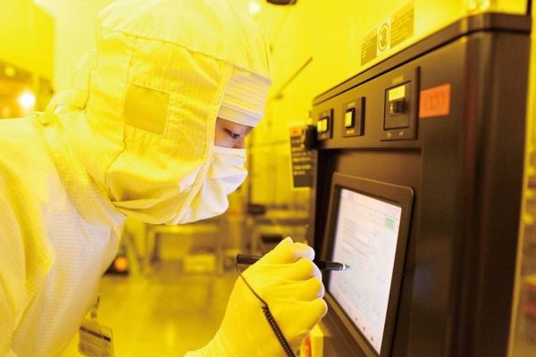
Automation in Photomask Inspection
Automation plays a crucial role in modern photomask inspection. Robotic systems ensure safe, consistent mask handling, minimizing human error and contamination. Automated scanning systems dynamically adjust inspection parameters based on mask complexity and defect sensitivity. Integration with fab operations allows for real-time feedback and process optimization. Automation also facilitates predictive maintenance, adaptive scanning, and continuous performance monitoring. By streamlining inspection workflows, automation improves throughput, maintains high-quality standards, and supports scalable semiconductor manufacturing globally.
Applications Across Semiconductor Devices
Photomask inspection is essential for semiconductor chips, MEMS devices, and display panels. Accurate masks ensure reliable device performance, high yield, and minimal defects. MEMS devices, including sensors and actuators, require precise pattern transfer for operational accuracy. Display panels such as LCD and OLED depend on defect-free masks for consistent image quality. R&D laboratories utilize advanced inspection systems to validate new lithography techniques, mask materials, and process optimizations. Global demand for smaller, faster, and more complex devices drives adoption of advanced, automated, and yield-focused inspection systems across semiconductor manufacturing sectors.
Data-Driven Process Optimization
Data-driven approaches enhance photomask inspection efficiency and yield. Inspection systems collect detailed data on defects, equipment performance, and production parameters. Analytics tools identify defect trends, root causes, and process inefficiencies, enabling proactive adjustments. Machine learning models predict potential yield loss and guide process optimization. Integration with fab operations ensures real-time feedback, adaptive scanning, and consistent production quality. Data-driven process optimization reduces rework, increases throughput, and maintains high-quality standards across semiconductor fabs globally, supporting efficient manufacturing and consistent product reliability.
Technological Advancements
Technological advancements in photomask inspection focus on yield improvement, advanced lithography, and equipment innovation. High-resolution imaging systems, AI-assisted defect detection, and automation optimize inspection performance. Robotics and automated handling reduce contamination and improve throughput. Predictive analytics allows proactive process adjustments, minimizing yield loss. Software platforms provide real-time reporting, trend analysis, and actionable insights. Continuous innovation ensures inspection systems can accommodate next-generation semiconductor nodes, complex mask designs, and high-volume production demands globally, supporting consistent quality and operational efficiency.
Market Drivers
The photomask inspection market is driven by several factors. Shrinking semiconductor nodes, increasing circuit complexity, and higher quality standards necessitate advanced inspection tools. Expansion of fabs worldwide increases demand for automated, high-resolution inspection solutions. Adoption of AI, predictive analytics, and yield improvement tools enhances efficiency, reduces defects, and optimizes production. Manufacturers benefit from improved throughput, lower operational costs, and higher product quality. Market growth is also supported by the increasing need for advanced logic chips, memory devices, sensors, and display technologies across global electronics markets.
Challenges
Despite growth, challenges remain. High investment costs may limit adoption of advanced inspection tools, particularly for smaller fabs. Increasing photomask complexity requires continuous technological upgrades. Skilled personnel are needed for system operation and analytics interpretation. Variability in defect detection accuracy can affect production consistency. Addressing these challenges requires AI-assisted defect analysis, user-friendly automation, comprehensive training programs, and vendor collaboration. Overcoming these hurdles ensures consistent inspection performance, higher yield, and efficient semiconductor manufacturing globally.
Future Outlook
The future of photomask inspection emphasizes yield improvement tools, advanced lithography, and equipment innovation. Real-time monitoring, predictive analytics, and AI-assisted inspection will define next-generation systems. Expansion of semiconductor fabs in Asia-Pacific, North America, and Europe will drive demand for advanced inspection solutions. Continuous innovation in inspection technology will ensure defect-free masks, optimized throughput, and improved yield. Companies investing in integrated, automated, and high-accuracy inspection systems will lead adoption. Photomask inspection will remain a critical enabler for efficient, reliable, and high-quality semiconductor manufacturing globally.


