
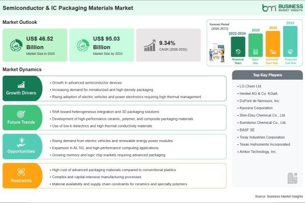
A substantial operational scale-up is redefining resin synthesis, high-precision substrate lamination, and automated encapsulation testing pipelines, fueled by the commercial necessity to achieve ultra-low warpage, superior heat dissipation, and optimal yield reliability for next-generation silicon packages worldwide.
Based on market intelligence from Business Market Insights, the global Semiconductor & IC Packaging Materials Market is anticipated to reach US$ 95.03 Billion by 2033, mounting from its 2025 value of US$ 46.52 Billion at a projected CAGR of 9.34% from 2026 to 2033.
Growth in advanced semiconductor devices, expansion of AI, 5G, and high-performance computing, and the need for thermal management and heterogeneous integration are key drivers. Asia-Pacific leads due to strong semiconductor manufacturing, while North America and Europe focus on innovation and advanced packaging.
Download Sample Report : https://www.businessmarketinsights.com/sample/BMIPUB00034320
What Are Semiconductor & IC Packaging Materials?
Semiconductor & IC Packaging Materials are specialized components used to protect, interconnect, and enhance the performance of integrated circuits and semiconductor devices. They include organic substrates, bonding wires, lead frames, encapsulation resins, solder balls, and thermal interface materials.
These materials ensure reliability, thermal management, electrical performance, and miniaturization in modern electronics.
Market Drivers
A primary driver is the growth in advanced semiconductor devices. Demand for AI chips, high-performance computing, and 5G infrastructure requires sophisticated packaging materials for heat dissipation, high-density integration, and reliability.
Expansion of electric vehicles, consumer electronics, and data centers further fuels demand for advanced packaging solutions that support miniaturization and performance.
Market Segmentation
By Type
- Organic Substrate: The dominant segment, offering cost-efficiency and high-density interconnect capability.
- Bonding Wires
- Lead Frames
- Encapsulation Resins
- Others
By Packaging Technology
- Grid Array: The leading segment, enabling high I/O counts and efficient heat dissipation.
- Small Outline Package
- Quad Flat Packages
- Others
By End Use
- Consumer Electronics: The dominant segment, driven by high-volume demand in smartphones, wearables, and home devices.
- Automotive
- Aerospace & Defense
- IT & Telecommunication
- Others
Regional Insights
- North America is a leading region due to advanced semiconductor ecosystem, R&D, and demand for high-performance packaging.
- Asia-Pacific shows strong growth with major manufacturing hubs in China, Taiwan, South Korea, and Japan.
- Europe focuses on innovation and sustainability in packaging materials.
Top Players in the Semiconductor & IC Packaging Materials Market
The market features leading chemical, materials, and packaging technology companies.
- LG Chem Ltd.
- Henkel AG & Co. KGaA
- DuPont de Nemours, Inc.
- Kyocera Corporation
- Shin-Etsu Chemical Co., Ltd.
- Sumitomo Chemical Co., Ltd.
- BASF SE
- Toray Industries Corporation
- Texas Instruments Incorporated
- Amkor Technology, Inc.
Technological Innovations
Manufacturers are developing advanced substrates, high-performance solders, thermal interface materials, and solutions for heterogeneous integration, 3D stacking, and fan-out packaging. Sustainability and environmental compliance are key focus areas.
Future Market Outlook
The Semiconductor & IC Packaging Materials Market outlook is highly positive through 2033, driven by AI, 5G, EV, and advanced computing trends. Continued innovation in advanced packaging will support miniaturization, performance, and sustainability in the semiconductor industry.
Frequently Asked Questions (FAQs)
What is the projected size of the Semiconductor & IC Packaging Materials Market by 2033?
The market is projected to reach US$ 95.03 Billion by 2033, rising from US$ 46.52 Billion in 2025.
What is the CAGR for the Semiconductor & IC Packaging Materials Market?
The market is expected to grow at a CAGR of 9.34% from 2026 to 2033.
Which type segment is dominant?
Organic Substrate holds the largest share due to cost-efficiency and high-density interconnect capability.
Which end use segment leads the market?
Consumer Electronics dominates due to high-volume demand in smartphones and other devices.
What is the primary factor driving demand?
The primary drivers are growth in advanced semiconductor devices, AI, 5G, EVs, and the need for high-performance, miniaturized packaging solutions.
Browse More Reports:
https://www.businessmarketinsights.com/reports/sustained-release-coatings-market
https://www.businessmarketinsights.com/reports/system-on-chip-market
https://www.businessmarketinsights.com/reports/technical-enzymes-market
About Us
Business Market Insights is a market research platform that provides subscription service for industry and company reports. Our research team has extensive professional expertise in domains such as Electronics & Semiconductor; Aerospace & Defense; Automotive & Transportation; Energy & Power; Healthcare; Manufacturing & Construction; Food & Beverages; Chemicals & Materials; and Technology, Media.
Contact Us
If you have any questions about this report or would like further information, please contact us:
Contact person: Ankit Mathur
Email: sales@businessmarketinsights.com
Phone: +16467917070