
A significant operational scale-up across wafer-level chemical synthesis, ultra-pure resin formulations, and fine-pitch leadframe stamping is prioritizing warpage reduction, thermal expansion co-efficient (CTE) matching, moisture sensitivity level (MSL) compliance, and zero-defect quality control.
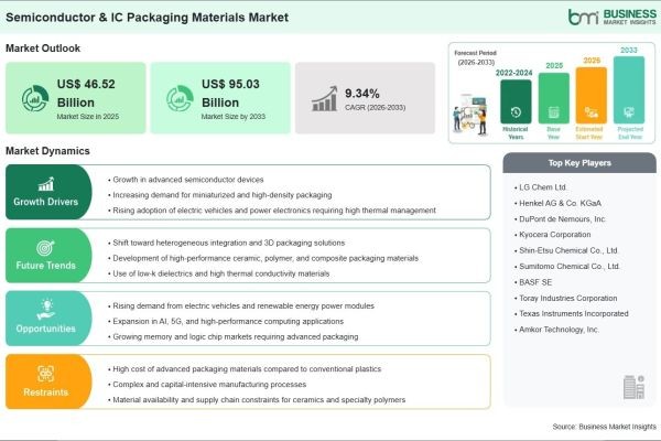
Based on market intelligence from Business Market Insights, the global Semiconductor and IC Packaging Materials Market [https://www.businessmarketinsights.com/reports/semiconductor-and-ic-packaging-materials-market] is anticipated to reach US$ 95.03 Billion by 2033, mounting from its 2025 value of US$ 46.52 Billion at a projected CAGR of 9.34% from 2026 to 2033.
Technological advancement is continuously shaping the industry landscape, with major chemical and material manufacturers focusing on high-density organic substrates, ultra-thin bonding wires, low-stress encapsulation resins, and advanced thermal interface materials (TIMs). Innovations in fan-out wafer-level packaging (FOWLP) and glass substrates are enabling superior interconnection density. Strategic investments in domestic semiconductor manufacturing and OSAT (Outsourced Semiconductor Assembly and Test) expansion are accelerating the deployment of these next-generation packaging material solutions globally.
Download Sample Report : https://www.businessmarketinsights.com/sample/BMIPUB00034320
What Are Semiconductor and IC Packaging Materials?
Semiconductor and Integrated Circuit (IC) packaging materials are specialized chemical compounds, metals, polymers, and ceramic substrates engineered to enclose, protect, and interconnect semiconductor dies. These materials form the protective housing and electrical interconnections that transform delicate silicon chips into functional, durable microelectronic components ready for board assembly.
These highly specialized materials are fundamental to demanding applications where signal performance, power distribution, and thermal management are non-negotiable. They encompass a broad range of products, including organic substrates, leadframes, bonding wires, die-attach adhesives, encapsulation molding compounds, solder balls, and thermal interface materials deployed across consumer, industrial, automotive, and defense electronics.
Market Drivers
A primary driver of the Semiconductor and IC Packaging Materials Market is the explosive rise of Artificial Intelligence (AI), high-performance computing (HPC), and cloud data center infrastructure. Processing modern AI workloads requires high-bandwidth memory (HBM) and complex multi-chip modules that demand high-density interposers, advanced substrates, and efficient thermal dissipation materials to handle extreme thermal densities.
The rapid electrification and digital transformation of the automotive industry act as another major catalyst. Advanced Driver Assistance Systems (ADAS), electric vehicle (EV) powertrains, and autonomous driving modules require high-reliability power semiconductors and sensor chips packaged with specialized materials capable of withstanding harsh operating temperatures, vibration, and environmental stress over extended operational lifespans.
Furthermore, the continuous trend toward device miniaturization in consumer electronics—such as 5G smartphones, smartwatches, and IoT endpoints—is accelerating market growth. The requirement to pack increased functionality, multi-band radio frequency components, and extended battery capacity into thinner devices drives intense demand for wafer-level packaging materials and System-in-Package (SiP) solutions.
RD URL: https://www.businessmarketinsights.com/reports/semiconductor-and-ic-packaging-materials-market
Market Segmentation
By Type
- Organic Substrates: The dominant and largest revenue-generating subsegment, favored for its high interconnect density, multi-layer wiring flexibility, and cost efficiency in flip-chip and BGA packaging.
- Bonding Wires: Crucial interconnect materials including copper, gold, silver, and aluminum alloys utilized extensively for leadframe-based packaging and high-volume IC assembly.
- Leadframes: Essential metal structures that provide mechanical support and external leads for traditional and surface-mount semiconductor packages.
- Encapsulation Resins & Molding Compounds: High-performance polymer formulations that shield delicate silicon dies from mechanical impact, moisture, and chemical contamination.
- Die Attach Materials & Thermal Interface Materials (TIMs): Specialized pastes, films, and liquid adhesives engineered for structural bonding and rapid heat dissipation.
- Ceramic Packages & Solder Balls: Highly reliable solutions used in aerospace, defense, and high-density ball grid array applications.
By Packaging Technology
- Flip-Chip Packaging: Widely adopted technology providing direct electrical connections via solder bumps, enabling higher signal speeds and compact form factors.
- Wafer-Level Packaging (WLP): A fast-growing segment where packaging operations are performed directly on the silicon wafer prior to dicing, offering minimal footprint.
- System-in-Package (SiP) & 3D Packaging: Advanced heterogeneous integration technique combining multiple heterogeneous ICs and passives into a single module.
- Traditional Surface Mount (BGA, QFN, SOP): Established high-volume packaging platforms used across standard consumer, industrial, and automotive electronics.
By End User
- Consumer Electronics: The largest end-use segment, driven by massive production volumes of smartphones, tablets, laptops, gaming consoles, and wearable devices.
- Automotive Electronics: High-growth segment fueled by EV power modules, infotainment ICs, battery management systems, and radar sensors.
- IT & Telecommunications: Driven by 5G base stations, networking switches, fiber-optic transceivers, and enterprise server processors.
- Industrial & Healthcare: Encompasses smart factory automation, power electronics, medical imaging devices, and diagnostic hardware.
- Aerospace & Defense: Specialized applications requiring radiation-tolerant, high-reliability ceramic and hermetic chip packages.
Regional Insights
- Asia-Pacific represents the dominant region and fastest-growing market. This leadership is underpinned by the world's largest semiconductor foundry ecosystem, major OSAT facilities, and dense electronics manufacturing bases across Taiwan, China, South Korea, Japan, and Southeast Asia.
- North America maintains a prominent market position, propelled by leading fabless chip designers, heavy AI datacenter investments, and federal initiatives such as the U.S. CHIPS Act to rebuild domestic packaging capabilities.
- Europe holds a significant market share, supported by a strong automotive semiconductor sector, advanced industrial electronics manufacturing, and strict regional environmental and chemical compliance frameworks.
- Middle East & Africa is experiencing steady growth, driven by digital infrastructure expansion, smart grid initiatives, and expanding telecom network installations.
- South & Central America is witnessing gradual market expansion as regional telecommunications infrastructure updates and consumer electronics assembly lines continue to grow.
Top Players in the Semiconductor and IC Packaging Materials Market
The competitive landscape features globally recognized chemical conglomerates, specialized substrate fabricators, and advanced materials providers focused on meeting stringent microelectronics requirements.
- Kyocera Corporation
- DuPont de Nemours, Inc.
- Henkel AG & Co. KGaA
- Shin-Etsu Chemical Co., Ltd.
- Sumitomo Bakelite Co., Ltd.
- Resonac Holdings Corporation
- ASE Technology Holding Co., Ltd.
- Mitsui High-Tec, Inc.
- Tanaka Kikinzoku Group
- STATS ChipPAC (JCET Group)
Technological Innovations
The shift toward 2.5D/3D heterogeneous integration and glass substrate technologies represents a transformative technological milestone in semiconductor packaging. As traditional silicon interposers face scaling and cost constraints, glass substrates offer superior thermal stability, lower electrical loss, and extreme planarity, enabling higher density interconnects required for next-generation AI processors and high-capacity memory stacks.
Additionally, the development of environmentally compliant, halogen-free, and low-VOC molding resins is accelerating in response to global environmental regulations like REACH and RoHS. Materials manufacturers are actively introducing novel epoxy formulations that feature lower curing temperatures, reduced thermal expansion coefficients, and enhanced moisture resistance to optimize yield rates during advanced high-density chip assembly.
Future Market Outlook
The future outlook for the Semiconductor and IC Packaging Materials Market remains highly lucrative through 2033. As physical limits on traditional transistor scaling make pure front-end miniaturization increasingly costly, semiconductor innovation is shifting decisively toward back-end advanced packaging solutions to achieve performance gains.
Market leaders over the next decade will be companies that can deliver customizable, high-purity materials optimized for chiplet architectures, hybrid bonding, and extreme thermal management while maintaining robust, resilient global supply chains.
Industry Snippet URL: https://www.businessmarketinsights.com/industry-overview
Frequently Asked Questions (FAQs)
What is the projected size of the Semiconductor and IC Packaging Materials Market by 2033?
The global market is projected to reach US$ 95.03 Billion by 2033, expanding from US$ 46.52 Billion in 2025.
What is the CAGR for the Semiconductor and IC Packaging Materials Market?
The market is estimated to record a steady CAGR of 9.34% during the forecast period from 2026 to 2033.
Which material type holds a dominant share in the market?
The organic substrates segment holds a major market share due to its widespread adoption in multi-layer flip-chip, BGA, and high-density IC applications.
Which region leads the global market?
The Asia-Pacific region dominates the global market, driven by the concentration of leading semiconductor foundries, OSAT providers, and electronics assembly hubs.
What are the primary drivers of market expansion?
Key drivers include the rapid proliferation of AI and high-performance computing, the growth of automotive electrification (EVs and ADAS), and the transition toward 2.5D/3D heterogeneous chip packaging.
Browse More Reports:
parking reservation system market [https://www.businessmarketinsights.com/reports/parking-reservation-system-market]
pedicle screw systems market [https://www.businessmarketinsights.com/reports/pedicle-screw-systems-market]
perovskite solar cell market [https://www.businessmarketinsights.com/reports/perovskite-solar-cell-market]
About Us
Business Market Insights is a market research platform that provides subscription service for industry and company reports. Our research team has extensive professional expertise in domains such as Electronics & Semiconductor; Aerospace & Defense; Automotive & Transportation; Energy & Power; Healthcare; Manufacturing & Construction; Food & Beverage; Chemicals & Materials; and others.
Contact Us
If you have any questions about this report or would like further information, please contact us:
Contact person: Ankit Mathur
Email: sales@businessmarketinsights.com
Phone: +16467917070